Memory BIST & Boundary Scan: Innovations for High-Density, AI-Driven Devices
Introduction
As memory densities soar and AI-driven applications proliferate, the need for robust memory Built-In Self-Test (BIST) and boundary scan solutions has never been greater. These technologies ensure the reliability and quality of modern electronic systems, from smartphones to data centers.
Memory BIST: Meeting the Challenges of Modern Memory
Memory BIST automates the testing of embedded and standalone memories, providing comprehensive coverage with minimal manual intervention.
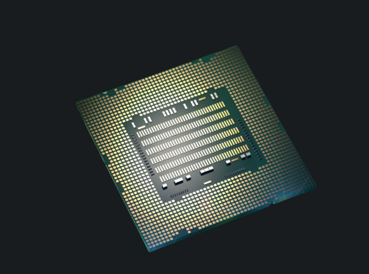
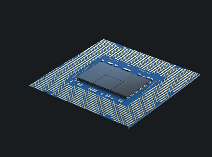
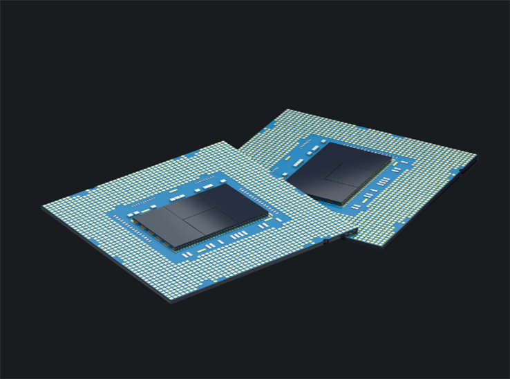
Support for High-Density Memories: Advanced BIST architectures handle DRAM, NAND, and 3D memory structures.
Speed and Efficiency: Automated test pattern generation accelerates testing, critical for high-volume manufacturing.
Boundary Scan: Ensuring Board-Level Quality
Boundary scan, standardized as IEEE 1149.1, enables the testing of interconnects on printed circuit boards (PCBs) without physical probes.
AI-Enhanced Diagnostics: AI tools analyze boundary scan data to quickly identify defects and predict failure trends.
Support for Complex PCBs: Modern boundary scan solutions handle high-speed interfaces and dense board layouts.
Trends and Innovations
Integration with AI: AI-driven diagnostics and pattern analysis improve accuracy and speed.
Support for HBM and Emerging Memory: New standards and tools address the unique challenges of high-bandwidth memory and other emerging technologies.
Market Outlook
The demand for memory BIST and boundary scan solutions is set to grow as devices become more complex and quality requirements tighten.
Conclusion
Innovations in memory BIST and boundary scan are vital for ensuring the performance and reliability of next-generation electronic systems. Companies that invest in these technologies will be well-positioned to meet the challenges of the AI era.
Powered by Froala Editor